GaN Solution
GaN FET Driver
uP1969
Dual-Channel Gate Driver for Enhancement Mode GaN Transistors
Datasheets PDF
General Description
The uP1969 is designed to drive both high-side and low-side enhancement mode Gallium Nitride (GaN) FETs in half bridge or synchronous buck configuration. The uP1969 has two PWM inputs which are utilized to independently control high-side and low-side drive signals. This part has under voltage lockout function for VCC power input. The floating high-side driver is capable of driving a high-side GaN FET operating up to 100V DC. This device employs bootstrap technique to provide power for the high-side driver. The bootstrap charging mechanism is designed to avoid overcharging for the bootstrap capacitor during switching dead time. Therefore, the gate to source voltage of GaN FET is prevented from exceeding its maximum rating. The uP1969 has split gate outputs to provide flexibility in adjusting both turn on and turn off strength independently.
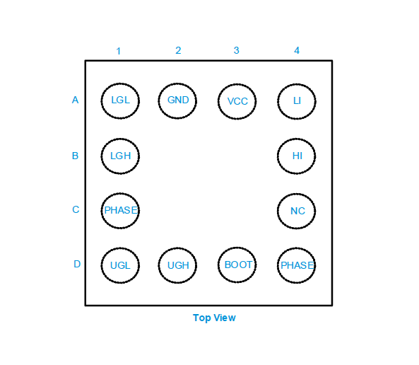
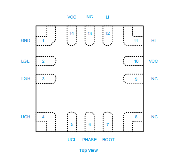
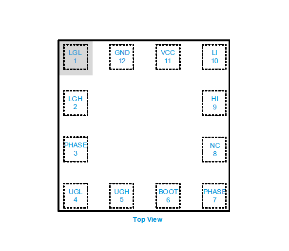
The uP1969 is available in three packages, WLCSP1.6×1.6-12B, VQFN3x3-14L (flip-chip) and UQFN2x2-12L (flip-chip) packages.
The uP1969 is available in three packages, WLCSP1.6×1.6-12B, VQFN3x3-14L (flip-chip) and UQFN2x2-12L (flip-chip) packages.
Pin Configuration & Typical Application Circuit

Integrated Driver / Isolator IC for H-B